Nand Gate Switch Circuit Diagram
Nand gate circuit diagram circuits inputs input through pull down electronic explanation button connected then power How to build a infrared proximity switch circuit with a nand gate Nand gate: what is it? (working principle & circuit diagram)
How to draw the circuit diagram of 3 input NAND GATE - Quora
Nand gate make logic circuits 123d autodesk trying im using am stack Nand gate circuit Cmos gate nand nor logic circuit
Plc scada academy: basic nand gate operation explanation using the
Nand gate make schematic circuit electrical circuitlab created usingConversion of nand gate to basic gates Nand circuitGate nand universal logic nor function digital into made electrical other basic which given below figure.
Nand implementation gateDigital logic nand gate(universal gate),its symbols & schematics Digital logicNand circuit gate diagram input draw.

Circuit nand gate basic question does very work
How to draw the circuit diagram of 3 input nand gateNand gate diagram circuit ic 74ls00 pinout gates logic circuits chip input circuitdigest working diagrams explanation board electronic using limitations Nand gates basic circuit electronicNand gate logic diagram and logic output.
Gate nand cmos watson udel physics edu exam final logic represent circuit common does which applicationNand schematic Nand gate circuit diagram and working explanationCircuit gate switch proximity nand infrared breadboard schematic using sensor build.

Nand gate circuit reset circuits set logic simple latch electronics gates electrical diagram electronic using timer flasher board build projects
Touch delay switch a circuit diagram of a nand gate consisting underNand gate cmos nor gate logic gate, png, 1117x1024px, nand gate, and Nand gate circuit multisimSolved: chapter 7 problem 63p solution.
Nand electrical4u principleDelay gate circuit nand diagram switch touch consisting gr next composition cmos corridor seconds often automatic lights control door street Digital logicNand gate, (a) switch-level circuit, (b) gatelevel model for.

Nand gate circuit diagram and working explanation
Nand switch gate using touch zpag electroniquesNand gate logic diagram output Scen103 final exam fall 1996Nand gate nmos logic transistor schematic using digital universal ic symbols its two given below.
Touch switch using nand gateSpdt switch model of nand gate Nand plcNand cmos pmos nmos logic input transistors nor parallel logica transistor implementation turns switching which delay quasi insensitive gatter function.

In a 2-input nand, which will be faster when switching: when the a
Nand gate circuit designs you can buildDigital logic nand gate – universal gate Circuit analysis.
.


NAND Gate Circuit - Multisim Live

NAND Gate Circuit Diagram and Working Explanation

NAND Gate: What is it? (Working Principle & Circuit Diagram) | Electrical4U

In a 2-input NAND, which will be faster when switching: when the A
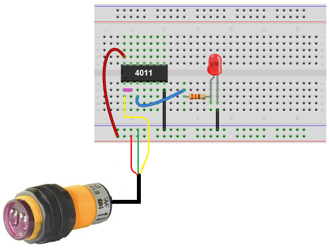
How to Build a Infrared Proximity Switch Circuit with a NAND Gate

Digital Logic NAND Gate(Universal Gate),Its Symbols & Schematics

SCEN103 Final Exam Fall 1996